Full Adder Circuit Diagram Explanation
Adder binary logic input sum output xor theorycircuit boolean diagrams derived following inputs Adder theorycircuit 8-bit adder circuit diagram
8 Bit Serial Adder Circuit Diagram
Full adder logic diagram Full adder circuit diagram Full adder in digital electronics
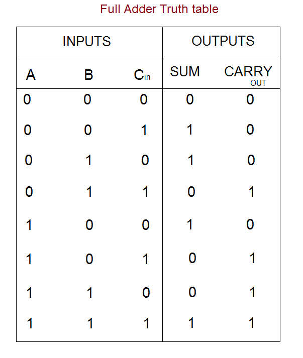
Adder truth table circuit full verilog code
Adder half adders circuits boolean circuit digital computer vhdl systems videoHow to design half adder and full adder circuits? Fulll adder circuit diagramImage gallery half adder.
Full adder circuit diagram using half adderFull adder circuit, truth table and verilog code Pin on electronic circuitsFull adder circuit diagram.

Full adder circuit diagram explanation
Adder full diagram circuit cin theorycircuit8 bit full adder circuit diagram Full adder circuit diagramHow to build a full adder circuit.
Adder half circuit full electronics diagram circuits engineering study4 bit full adder diagram Adder half circuit diagram gate block gates sum input digital two choose board circuits construction bit used carry bothBcd adder.

Adder logic block boolean
Build and simulate full adder circuit using half adder as a componentCircuit diagram of full adder 8 bit serial adder circuit diagramDifferentiate between half adder and full adder draw the logic circuit.
Full adder circuit diagramBcd adder 4 bit adder circuit diagramVhdl half adder.

[diagram] bcd adder circuit diagram
Adder logic pla inputs explainExplain half adder circuit with diagram .
.
![[DIAGRAM] Bcd Adder Circuit Diagram - MYDIAGRAM.ONLINE](https://i2.wp.com/www.electronicsengineering.nbcafe.in/wp-content/uploads/2014/09/full-adder.png)